前言简易数字频率计原理顶层控制模块:计数模块:锁存模块测试文件结语
前言
这篇博客大概是2017年写的,目前已经是2020年8月不到,今天维护了一下但是并未保存,很受伤,不得不重新在维护一次。
最近看到很多评论,说程序有问题,于是我就对这个程序进行一次测试。
并更新博文程序与其他部分内容。 个人博客以及知乎:李锐博恩 个人微信公众号:FPGA LAB
简易数字频率计原理
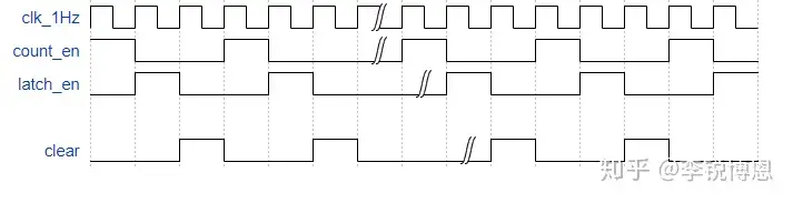
原理:数字频率计的原理十分简单,简单的就是一句话和一幅图而已。
一句话:测量被测信号的频率,要清楚频率的定义,一言以蔽之,就是1s中信号的周期数。
根据频率的定义,我们测量被测信号1s中变化的次数即可,即1s中的周期数。
首先我们设置一个基准时钟信号,频率为1Hz,从第一个上升沿开始计数(被测信号的上升沿数),直到下一个上升沿到达时停止计数,对数据进行锁存,再到达下一个上升沿时,对计数器进行清零,准备下一次的测量。
根据以上描述,得到相关信号的关系:
一幅图:
我尝试使用wavedrom画了这个图:
本图是简易频率计的工作时序图,从图中 可以看出:
基准信号的第一个上升沿到达时,计数使能信号有效,计数器开始计数;
第二上升沿到达时,计数结束,锁存使能有效,计数数据开始锁存;
第三个上升沿到达时,清零信号有效,对计数器的输出清零,准备下一次的测量。
一个测量过程需要3 sec(重要)。
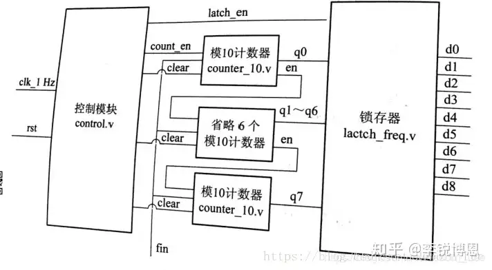
下面是数字频率计的原理图:
还没来得及使用visio更新! 由此原理图可以清晰的理解下面的verilog HDL程序:
程序可以分为四个部分,一个顶层模块,三个子模块:
顶层
`timescale 1ns / 1ps
//////////////////////////////////////////////////////////////////////////////////
// blog: https://blog.csdn.net/Reborn_Lee
// Engineer: 李锐博恩
// Design Name: frequency detect
// Module Name: freDetect
//
//////////////////////////////////////////////////////////////////////////////////
module freDetect(
input wire clk_1Hz, //1Hz基准频率,周期1s;
input wire fin, //输入待测信号
input wire rst, //复位信号
output wire [3:0] d0,
output wire [3:0] d1,
output wire [3:0] d2,
output wire [3:0] d3,
output wire [3:0] d4,
output wire [3:0] d5,
output wire [3:0] d6,
output wire [3:0] d7
);
wire [3:0] q0, q1, q2, q3, q4, q5, q6, q7; //中间数据
//控制模块实例
control control_inst(.clk_1Hz(clk_1Hz),
.rst(rst),
.count_en(count_en),
.latch_en(latch_en),
.clear(clear)
);
//计数器模块实例
counter_10 counter_inst0(.en_in(count_en),.clear(clear),.rst(rst),
.fin(fin),.en_out(en_out0),.q(q0));
counter_10 counter_inst1(.en_in(en_out0),.clear(clear),.rst(rst),
.fin(fin),.en_out(en_out1),.q(q1));
counter_10 counter_inst2(.en_in(en_out1),.clear(clear),.rst(rst),
.fin(fin),.en_out(en_out2),.q(q2));
counter_10 counter_inst3(.en_in(en_out2),.clear(clear),.rst(rst),
.fin(fin),.en_out(en_out3),.q(q3));
counter_10 counter_inst4(.en_in(en_out3),.clear(clear),.rst(rst),
.fin(fin),.en_out(en_out4),.q(q4));
counter_10 counter_inst5(.en_in(en_out4),.clear(clear),.rst(rst),
.fin(fin),.en_out(en_out5),.q(q5));
counter_10 counter_inst6(.en_in(en_out5),.clear(clear),.rst(rst),
.fin(fin),.en_out(en_out6),.q(q6));
counter_10 counter_inst7(.en_in(en_out6),.clear(clear),.rst(rst),
.fin(fin),.en_out(en_out7),.q(q7));
//锁存器模块实例
latch_freq latch_freq_inst(.clk_1Hz(clk_1Hz),.rst(rst),.latch_en(latch_en),
.q0(q0),.q1(q1),.q2(q2),.q3(q3),.q4(q4),.q5(q5),
.q6(q6),.q7(q7),.d0(d0),.d1(d1),.d2(d2),.d3(d3),
.d4(d4),.d5(d5),.d6(d6),.d7(d7));
endmodule
顶层模块例化了各种子模块:
控制模块:
`timescale 1ns / 1ps
//////////////////////////////////////////////////////////////////////////////////
// blog: https://blog.csdn.net/Reborn_Lee
// Engineer: 李锐博恩
// Design Name: frequency detect
// Module Name: control
//
//////////////////////////////////////////////////////////////////////////////////
module control(
input wire clk_1Hz,
input wire rst,
output reg count_en,
output reg latch_en,
output reg clear
);
reg[1:0] state; //状态信号,用于控制各种使能信号
always @(posedge clk_1Hz or posedge rst)
if(rst) //复位信号有效
begin //各种使能信号清零
state <= 2d0;
count_en <= 1b0;
latch_en <=1b0;
clear <= 1b0;
end
else //遇到基准信号的下一个上升沿,状态变化一次,每次变化后状态持续1s
begin
case(state)
2d0:
begin //第一个上升沿到达,开始计数,计数1个基准信号周期内待测信号的上升沿个数,此个数即为待测信号的频率
count_en <= 1b1; //计数使能信号有效
latch_en <=1b0;
clear <= 1b0;
state <= 2d1;
end
2d1:
begin //第二个上升沿到达,计数完成,锁存使能信号有效,测得频率锁存至锁存器中
count_en <= 1b0;
latch_en <=1b1;
clear <= 1b0;
state <= 2d2;
end
2d2:
begin //第三个上升沿到达,清零使能信号有效,计数器清零,为下一次计数做准备
count_en <= 1b0;
latch_en <=1b0;
clear <= 1b1;
state <= 2d0; //状态清零,进入下一次测量
end
default:
begin
count_en <= 1b0;
latch_en <=1b0;
clear <= 1b0;
state <= 2d0;
end
endcase
end
endmodule
计数模块:
`timescale 1ns / 1ps
//////////////////////////////////////////////////////////////////////////////////
// blog: https://blog.csdn.net/Reborn_Lee
// Engineer: 李锐博恩
// Design Name: frequency detect
// Module Name: counter_10
//
//////////////////////////////////////////////////////////////////////////////////
module counter_10(
input wire en_in, //输入使能信号
input wire rst, //复位信号
input wire clear, //清零信号
input wire fin, //待测信号
output reg en_out, //输出使能,用于控制下一个计数器的状态,当输出使能有效时,下一个模10计数器计数加1
output reg [3:0] q //计数器的输出,4位BCD码输出
);
always@ (posedge fin or posedge rst) //输入待测信号的上升沿作为敏感信号
if(rst) begin //复位信号有效,计数器输出清零
en_out <= 1b0;
q <= 4b0;
end
else if(en_in) begin //进位输入使能信号有效
if(q == 4b1001) begin //若q = 4b1001的话,q清零,同时进位输出使能有效,即en_out 赋值为1b1
q <= 4b0;
en_out <= 1b1;
end
else begin //若q未达到4b1001时,每到达待测信号的一个上升沿,q加1,同时输出进位清零
q <= q + 1b1;
en_out <=1b0;
end
end
else if(clear) begin //若清零信号有效,计数器清零,主要用于为下一次测量准备
q <= 4b0;
en_out <= 1b0;
end
else begin
q <= q;
en_out <=1b0;
end
endmodule
锁存模块
`timescale 1ns / 1ps
//////////////////////////////////////////////////////////////////////////////////
// blog: https://blog.csdn.net/Reborn_Lee
// Engineer: 李锐博恩
// Design Name: frequency detect
// Module Name: latch_freq
//
//////////////////////////////////////////////////////////////////////////////////
module latch_freq(
input wire clk_1Hz,
input wire latch_en,
input wire rst,
input wire [3:0] q0,
input wire [3:0] q1,
input wire [3:0] q2,
input wire [3:0] q3,
input wire [3:0] q4,
input wire [3:0] q5,
input wire [3:0] q6,
input wire [3:0] q7,
output reg [3:0] d0,
output reg [3:0] d1,
output reg [3:0] d2,
output reg [3:0] d3,
output reg [3:0] d4,
output reg [3:0] d5,
output reg [3:0] d6,
output reg [3:0] d7
);
always@ (posedge clk_1Hz or posedge rst)
if(rst) //复位信号有效时输出清零
begin
d0 <= 4b0; d1 <= 4b0; d2 <= 4b0; d3 <= 4b0; d4 <= 4b0;
d5 <= 4b0; d6 <= 4b0; d7 <= 4b0;
end
else if(latch_en) //锁存信号有效时,将计数器的输出信号锁存至锁存器
begin
d0 <= q0; d1 <= q1; d2 <= q2; d3 <= q3; d4 <= q4;
d5 <= q5; d6 <= q6; d7 <= q7;
end
else //上面两种情况均未发生时,输入不变
begin
d0 <= d0; d1 <= d1; d2 <= d2; d3 <= d3; d4 <= d4;
d5 <= d5; d6 <= d6; d7 <= d7;
end
endmodule
测试文件
`timescale 1ns/1ps
//测试模块
module freDetect_tb;
//为了仿真方便,全部缩小100倍;
parameter CLK_1HZ_DELAY = 1000_0000; //1Hz基准信号,对应周期为1s=1000_000_000ns
parameter FIN_DELAY = 2; //5MHz待测信号,对应周期为0.2*1000_000=200ns
reg clk_1Hz;
reg fin;
reg rst;
wire[3:0] d0, d1, d2, d3, d4, d5, d6, d7;
initial
begin
rst =1b1;
#1 rst = 1b0;
end
initial
begin
fin = 1b0;
forever
# (FIN_DELAY/2) fin = ~fin;
end
initial
begin
clk_1Hz = 1b0;
forever
# (CLK_1HZ_DELAY/2) clk_1Hz = ~clk_1Hz;
end
freDetect freDetect_inst(.clk_1Hz(clk_1Hz), .rst(rst), .fin(fin),
.d0(d0), .d1(d1), .d2(d2), .d3(d3), .d4(d4), .d5(d5), .d6(d6), .d7(d7));
endmodule
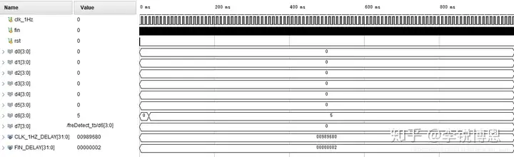
本仿真在vivado自带的仿真器进行行为仿真,使用其他仿真软件也可以,例如modelsim,本文使用vivado进行仿真,仿真结果如下:
我们设定的待测频率也是5Mhz=5000000Hz。
由于时间紧张,我就不具体展开中间变量了,大家自行分析。
结语
由于这篇博客时间有点长,csdn也经过了一些改版,导致早期的程序出现一些奇怪的字符,见博客:
网上复制代码需谨慎,莫名其妙报错看这里!
这恐怕也是广大看客直接复制我这篇文章代码所遇到的问题之一,不过现在这个问题解决了,大家可以再次尝试了。
免责声明:文章内容来自互联网,本站仅作为分享,不对其真实性负责,如有侵权等情况,请与本站联系删除。
转载请注明出处:简易数字频率计(verilog HDL设计)(2020维护版本) https://www.zentong.com/zt/9330.html